The Vacuum Spark – An Engineer's Nightmare!
It would not be an exaggeration to say that very few people are consciously aware of how much of our technical infrastructure depends on being able to reliably sustain a high electric field between a pair of metal electrodes in an high vacuum environment without a spark occurring, and the consequent breakdown of the electrical insulating capability of the vacuum gap. Examples of where such an event would be critical include our satellite communication systems, our national grid, medical diagnostics, and particle accelerators such as the LHC at CERN, all of which employ such vulnerable devices as travelling wave tubes, vacuum capacitors, vacuum switches and RF particle accelerating modules. Such is the importance of this subject, there are two international conferences focussed on it, the International Symposium on Discharges and Electrical Insulation in Vacuum (ISDEIV), and IEEE Conference on Electrical Insulation and Dielectric Phenomena.
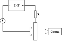
zsThe technical problem faced by all of the above industries is how to reliably suppress the “cold” or field emission of electrons from an extended metal surface which are responsible for triggering the formation of a spark between the electrodes, and the consequent electrical breakdown of the vacuum gap. This phenomenon can be readily demonstrated by using the simple experimental regime illustrated in the schematic below in which a gradually increasing voltage is applied across a plane-parallel vacuum gap consisting of a metal cathode and a glass anode coated with a semi-transparent conducting film that luminesces when impacted by high energy electrons. A high-speed camera can then be used to record any optical activity that occurs in the gap during this process.
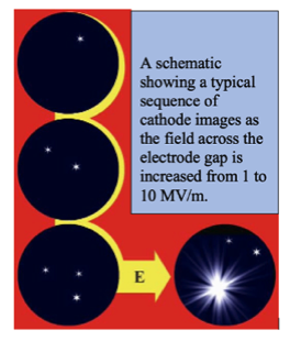
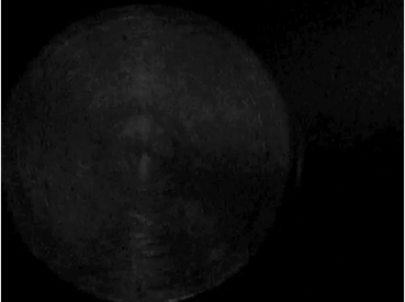
The above sequence, including the original video clip, illustrates how electron emission is initially confined to a microscopically localised “pre-breakdown” site which, at some critical field, becomes unstable, explodes in the form a spark, and results in the proliferation of a second generation potentially unstable emission sites. In practical terms, this represents an irreversible degrading of the electrical insulating capability of the vacuum gap.
The field-induced, or “cold”, emission of electrons has traditionally been attributed to the Fowler-Nordheim quantum mechanical tunnelling mechanism, and has been extensively researched in the context of the pointed-tip cathode regime used in field emission microscopy where the applied field is ~109 V/m. In contrast, the field at which the phenomenon occurs with an extended planar electrode geometry is typically two orders of magnitude lower, indicating that a different physical mechanism must be responsible for the electron emission. In fact, a range of dedicated diagnostic techniques established that the emission was associated with the presence of microscopic impurity particles, typically carbon, that are either adhering to, or embedded in the electrode surface, and giving rise to a complex semiconductor-based emission mechanism.
This discovery subsequently led to a revolution in high voltage engineering involving the introduction of clean-room technology, and the development of high-purity electrode materials which, together, have resulted in a progressive increase in the breakdown field that can be achieved with large-area high-voltage vacuum gaps. This sea change in approach has also revealed that there is a hierarchy in the materials most suited for use as high volage electrodes, with titanium and tantalum being the best, with copper and nickel being the worst. This finding therefore posed the challenge of providing a physical explanation for this behaviour.
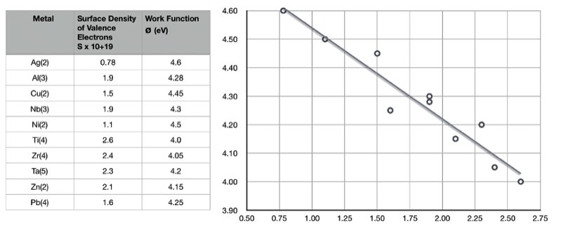
In this context, a recent analysis has shown, as illustrated in the plot below, that there is an inverse linear relationship between the work function of a surface and the surface density of its valence electrons S.
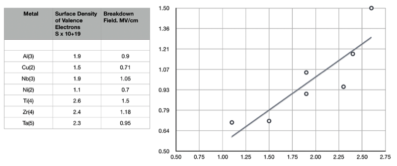
Subsequently, it was shown, as illustrated by the plot below, that there is an increasing linear relationship between the breakdown field and the S-parameter. This finding has practical implications, but it remains to determine how the S parameter influences the high-field emission of electrons.
Further details of the above phenomena can be found elsewhere on this site.